UV Photonics Research#
A partial picture of UV photonic device research (LEDs & FP-EELDs)#
UV photonic devices utilize AlGaN (Aluminum Gallium Nitride) crystal (both a ZincBlende and Wurtzite) to achieve the generation of photons at the wavelength of 200nm to 350nm. Different regions of UV spectrum may have different growth technique, and each region in the spectrum has its challenges. See Fig. 5 for reference.
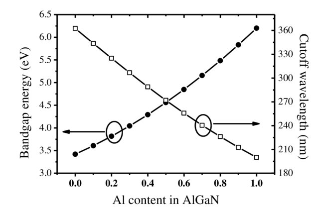
Fig. 5 Change in Al content in \(\text{Al}_\text{x}\text{Ga}_{\text{(1-x)}}\text{N}\) results in widening the optical bandgap, which results in emitting photons of shorter wavelength. Graph from [SLS13].#
One of the biggest challenges in UV-A LED research is in growing AlGaN on top of AlN/Sapphire due to large lattice mismatch between GaN and AlN. If the lattice mismatch is too great, cracks may be observed on the crystal as a result of great tensile strain. Note also that Al lattice constant and Ga lattice constant expand at different temperatures, and along different orientations of the plane (think Miller Indicies) the thermal expansion of lattice constant differs as well, all of which adds to the challenge of finding ideal growth conditions in terms of how strained and relaxed the crystal lattice should be. [Zol+21] Another challenge in UV photonics research as a whole is the fact that UV wavelength of light is not transparent to GaN (n = 2.5), due to Total Internal Reflection (TIR) where light gets trapped in the cladding layer[Wei+20], hence a low External Quantum Efficiency as a result of Light Extraction Efficiency (LEE) suffering a huge loss. This is especially true further into Deep UV wavelength – high p-GaN absorption of UV radiation is exhibited. This is the exact reason why a flip chip design for UV LEDs are used – light rays exit from the n-AlGaN side.
Characterization methods:#
Characterization is instrumental in modelling growth trend and monitoring growth result. Without characterization, there would be no data to study from. The tools used for characterization include but are not limited to High Resolution X-Ray Diffraction (HRXRD), Atomic Force Microscopy, Scanning Electron Microscopy, Photoluminescence Test, quick test and Hall Measurements.
X-Ray Diffraction:#
XRD is performed to generate what is called a Reciprocal Space Map in <105> plane, which works to parameterize the growth condition of the AlGaN crystal in momentum/reciprocal space. (Or you can say \(\hbar=1\), \(\hbar a\hbar a\).) The diffractometer is also capable of characterizing the samples in other ways, such as the rocking curve, and others.
Reciprocal Space Map (RSM) Analysis for AlGaN:#
The following description of Reciprocal Space specifically addresses AlGaN only:
Along the vertical axis (\(p_z\)) gives you the Al-content. The further up top along \(p_z\), the higher Al-content; the lower along \(p_z\), the more Ga-content.
Along the horizontal axis (\(p_x\)) tells you the lattice constant of the AlGaN crystal.
The crystal may or may not have a narrow stream of intensity. In which case, if the crystal follows along a straight line pointing downward, the crystal is strained, meaning the interface between different layers of different AlGaN composition are neatly aligned, with minimal defects. Keep in mind that defects may or may not be a bad thing. (Sometimes annealing can help)
In Fig. 6, it mentions Poisson’s effect, and you should not feel intimidated by the word “Poissons”. To give an example, if you have been given a cubic lattice, at the level of Bravais lattice, you can simply think of the crystal as a cube. All that Poisson’s effect is saying is that upon lattice mismatch, the crystal has been stretched from a cubic lattice into a rectangular lattice, while its total volume remains unchanged. Such is the ideal case for a perfectly strained lattice. But is reality perfect?
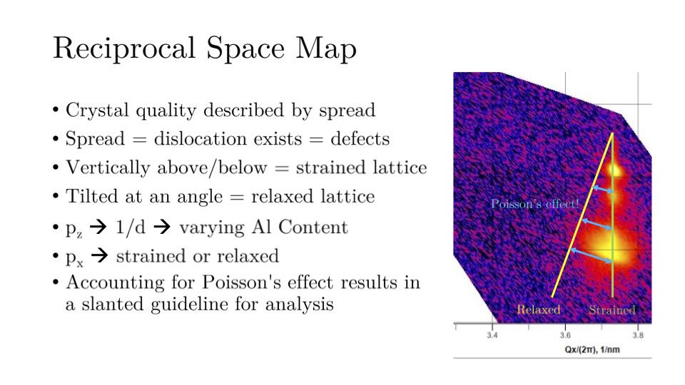
Fig. 6 RSM Justification.#
Rocking Curve Analysis for AlGaN:#
The following description of Rocking Curve specifically addresses AlGaN only:
The Full-Width-Half-Max (FWHM) of the rocking curve for (002) plane and (102) plane in an \(\omega\) scan tells you the crystal quality. The same spread has some correspondance to the spread of the Reciprocal Space Map, which indicates relaxed lattice, and its mosaicity (how ordered the crystal lattice is macroscopically speaking) can be poor. In other words, if the FWHM of the bell peak is narrow, the crystal quality could be decent, which is an indication of decent mosaicity.
Atomic Force Microscopy:#
Atomic Force Microscopy is used to characterize surface morphology of crystals. It provides another perspective on the roughness of the crystal. It is capable of analyzing the epitaxial layers’ surfaces. AFM pictures can be interesting and simply entertaining to look at, because the pictures are at a micron scale (\(10^{-6}\) or \(\mu m\))
AFM Analysis for AlGaN:#
Images are typically taken in sizes of 20x20 μm\(^2\), 5x5 μm\(^2\), and 2x2 μm\(^2\). One of the parameters of the image would be RSM roughness, and it tells you if the epitaxial layer is just rocky enough, too rocky, or too smooth and lacking atomic steps. It can affect the layers grown on top and provides a more physical and immediate detail on the alignment of the different epitaxial layers. This is why AFM is done on n-layers, MQW and p-layers, etc. From time to time, one would also need to do an AFM scan on the LED device to see if it can work well with the tunnel junction. By experience, one can deduce a few things from doing AFM scans:
Note
If the roughness is too strong, the layers grown on top can misalign in terms of the discussion of lattice plane, resulting in the collapse of any layers grown on top. It may or may not be an indicator of relaxed lattice.
In an LED, strong Root-Mean-Squared (RMS) surface roughness of the n-AlGaN layers can result in the collapse of quantum well alignment in the active regions, causing the crystal to fail.
In an Edge Emitting Laser where waveguides/cladding layers are used, poor RMS surface roughness can be a factor that affects the stability of guided modes, resulting in unstable transverse mode hopping (\(\text{TEM}_{nm}\)) unrelated to longitudinal mode hopping, or longitudinal gain (intensity vs. wavelength). It is also accountable for the light extraction efficiency loss. see Fig. 7 for an image example.
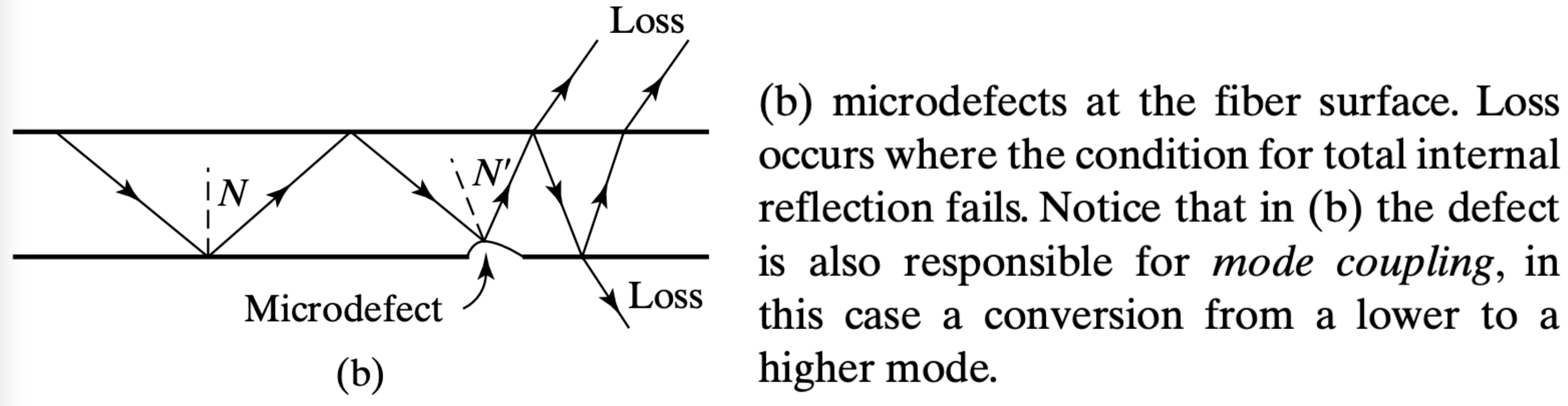
Fig. 7 Discussion of microdefects in the discussion of attenuation and Fiber Optics from chatper 10 of Introduction to Optics 3rd Ed. by Pedrotti.[PPP17] While the topic differs slightly, the concept still applies in terms of applying Snell’s law and Total Internal Reflection in the discussion of a waveguide.#
If the roughness is too smooth, it is typically a good indicator, which results in easier growth for layers on top. But too smooth could also be an indicator of lacking atomic steps.
See the images attached for AFM images
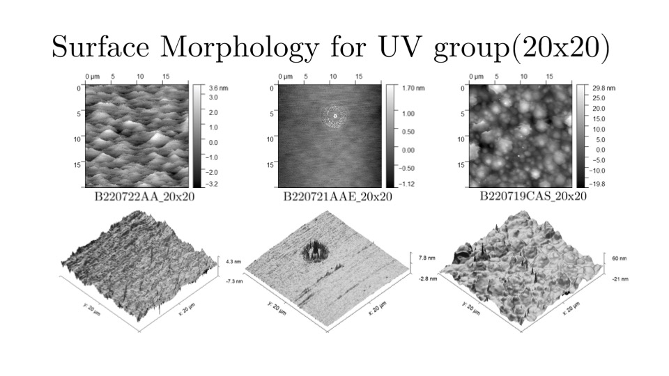
Fig. 8 AFM Images for epi layers at size 20um x 20um#
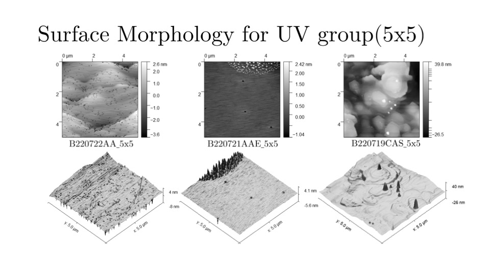
Fig. 9 AFM Images for epi layers at size 5um x 5um#
How do you do AFM scans?#
load the tip onto the mount.
load the mount onto the MFP3D.
An external camera is used to observe the behavior of the tip. The task to do now is to adjust the Rx and Ry position of the tip, which locates the tip directly on top of the epitaxial substrate.
On top of that, align the laser within the MFP3D directly on the tip. Doing this means you are maiximizing the sum.
Minimize the deflection, which means that the photodetector senses the laser appropriately.
Engage and autotune the tip such that the computer generates a graph showing that the tip is working.
Adjust the scan rate, amplitude, voltage, Integral Gain, and size of the images accordingly.
Typically, when doing AFM for epitaxial substrates, non-contact mode is used. In physics language, non-contact mode means that the AFM device utilizes the non-contact portion of Lennard-Jones potential. Lennard Jones Potential is a non-bonding atomic force felt between the two different “molecules” (between the tip and the substrate). Refer to Fig. 10 for an image summary.
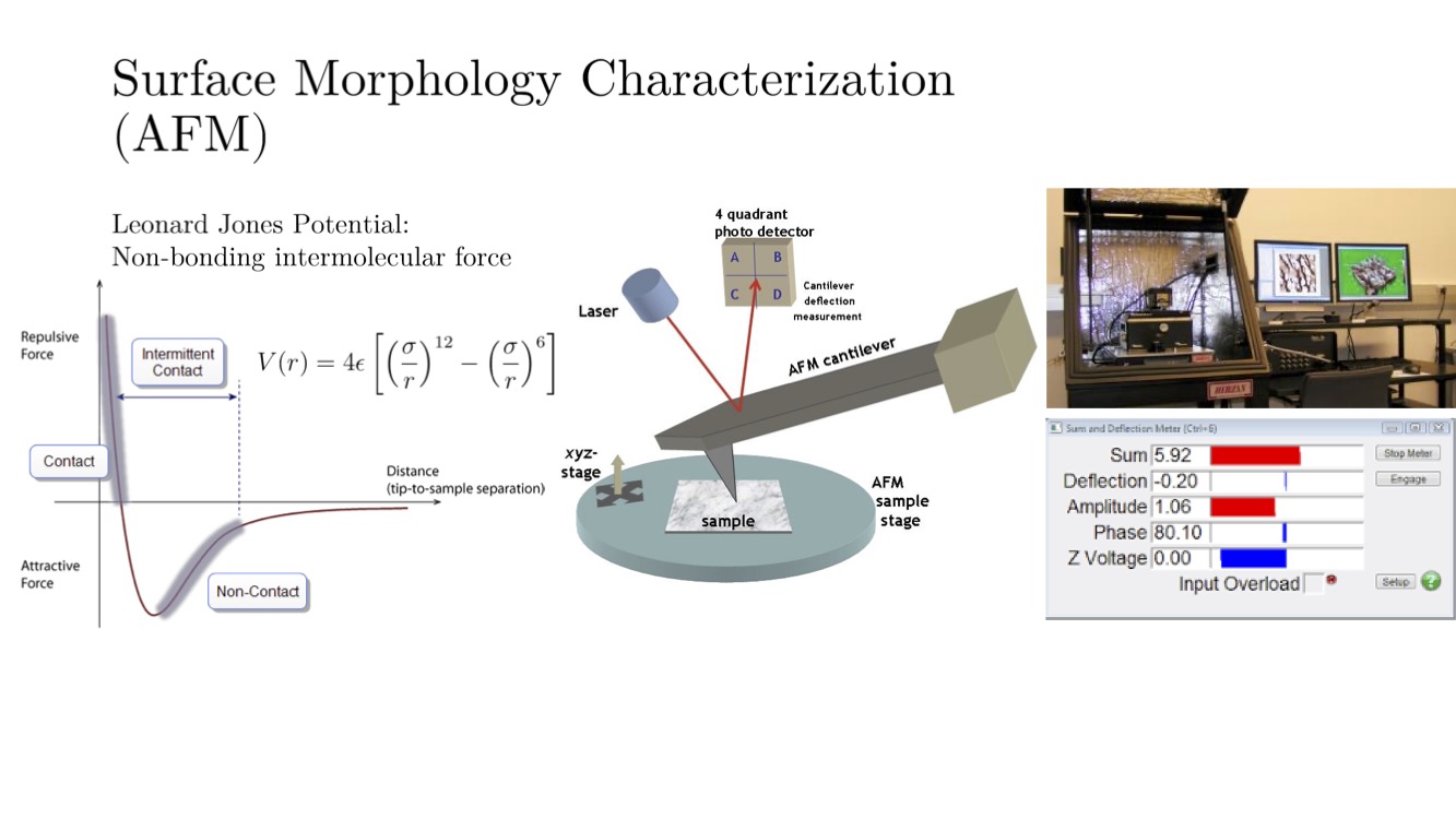
Fig. 10 Lennard Jones Potential, AFM setup, MFP3D! Images are found on google!#
For more detailed procedures, check out the manual published by Oxford Instrument Asylum Research.
How far into the future will an AlGaN UV-VCSEL be achieved:#
Since LEE of UV wavelength is low due to Total Internal Reflection, where light gets trapped in the guided modes, the build of a Fabry Perot Edge Emitting Laser (EEL) is a more feasible solution simply from the standpoint of ray tracing. A Distributed Feedback (DFB) Grated EEL would be an expensive build due to difficult fabrication of the Bragg’s grating at an atomic level (think in terms of Miller Indicies).
The only way to generate a truly fundamental \(\text{TEM}_{00}\) mode is through a Vertical Cavity Surface Emitting Laser (VCSEL), but light has to come out through the top and bottom of the device, when LEE (referring to an LED, think in terms of ray tracing) is extremely low. When do you think a UV FP-VCSEL will be achieved (within the immediate future/ or far into another decade or two)?
One of the greatest achievements in the History of Science from 30 years ago:#
30+ years ago, everyone believed that ZnSe (II-VI materials) would have been the ideal materials which can give rise to the invention of blue and white LED based on theoretical calculations, and everyone believed that Gallium Nitride Research would have been equivalent to “walking in wasteland” given the difficulty of the research. The only ones in the field doing research in III-Nitride materials back in the late 80s were only Dr. Hiroshi Amano, Dr. Isamu Akasaki and Dr. Shuji Nakamura.
Amano and Akasaki’s achievement were in developing a research grade MOVPE system to successfully grow GaN on Sapphire, and they provided a big hint for how ideal growth result should be – a mirror-like gloss on its surface. Prior to that, they derived the idea to grow Mg-doped GaN samples from a paper published in 1972 by H.P. Maruska, a PhD student at the time from Stanford University. Maruska published a paper which documented the invention of Metal-Insulator-Semiconductor (MIS) type Mg-doped GaN based violet LED using Hydride Vapor Phase Epitaxy (HVPE). This motivated Amano and Akasaki to grow p-GaN by doping the crystal with Mg using Metal Organic Vapor Phase Epitaxy (MOVPE).
Later, Amano and Akasaki together realized a post-growth Low Energy Electron Beam Irradiation (LEEBI or E-Beam) treatment, which allowed for an increase in conductivity of p-GaN film, but the reasoning was yet to be justified. Shortly after the discovery of post growth E-beam treatment, Nakamura published two papers documenting alternatives to E-beam treatment as well as the physical justification of hole compensation mechanism, with an improved and much more efficient method to achieve p-GaN conduction.
Dr. Shuji Nakamura’s achievement was not only in modifying an MOCVD reactor for GaAs into a two-flow MOCVD system suitable for GaN, which sprays \(\text{N}_2 + \text{H}_2\) gas through the secondary flow (antiperpendicular to surface) to press the main gas flow (which is parallel to surface) downward onto the substrate.
He also provided a much more efficient solution to annihilate (or passivate) the Hydrogen that was bonded to the Mg through \(\text{N}_2\)-ambient annealing, with which the Mg-H complex prevented the p-GaN from acting as an acceptor. Upon post-growth \(\textbf{N}_2\)-ambient thermal annealing at temperatures above 700˚C, p-GaN resistivity/conductivity is greatly decreased/increased by almost 6 orders of magnitude (from \(10^6\text{ }\Omega\cdot\text{cm}\) to \(10^0\text{ }\Omega\cdot\text{cm}\)).[Nak+92b] Note that the atomic Hydrogen came from \(\text{NH}_{3(g)}\), with \(\text{NH}_{3(g)}\) acting as a precursor for one of the chemical reactions in the MOCVD system.
Thermal Annealing is also an easily “commercialized” process that every manufacturing company adopted this method to achieve increase in conductivity. Nakamura soon published another paper documenting and identifying the atomic Hydrogen acting as a acceptor blocker (Mg-H complex) through annealing with \(\textbf{NH}_{3(g)}\), and that the effects of annealing is reversible by annealing again with \(\textbf{N}_{2(g)}\).[Nak+92a] The hole compensation mechanism experiment provided the first proposition for future theoretical calculation and the proposition of hydrogen passivation was later confirmed theoretically by Chris G. Van de Walle, et al in 1995.[NV95] This allowed for the creation of a p-n junction, where the p-GaN is conductive enough and polarized enough with respect to n-AlGaN to make a semiconductor diode out of it.
References#
Working on the reference now, the outline of the whole page is in progress also as I attempt to implement the bibliography import automation.
[Nak+92a] Shuji Nakamura et al. “Hole compensation mechanism of p-type GaN films”. In: Japanese Journal of Applied Physics 31.5R (1992), p. 1258.
[Nak+92b] Shuji Nakamura et al. “Thermal annealing effects on p-type Mg-doped GaN films”. In: Japanese Journal of Applied Physics 31.2B (1992), p. L139.
[NV95] Jörg Neugebauer and Chris G Van de Walle. “Hydrogen in GaN: Novel aspects of a common impurity”. In: Physical review letters 75.24 (1995), p. 4452.
[SLS13] Liwen Sang, Meiyong Liao, and Masatomo Sumiya. “A comprehensive review of semiconductor ultraviolet photodetectors: from thin film to one-dimensional nanostructures”. In: Sensors 13.8 (2013), pp. 10482–10518.
[PPP17] Frank L Pedrotti, Leno M Pedrotti, and Leno S Pedrotti. Introduction to optics. Cambridge University Press, 2017.
[Wei+20] C. Weisbuch, H. Benisty*, M. Rattier*, D. Labilloy*, A. David, E. Matioli, C. Lalau-Keraly, M. Cochet, and L. Kuritzky. “Light Extraction in Nitride LEDs”, https://www.energy.gov/sites/default/files/2020/02/f71/ssl-rd2020-weisbuch-extraction.pdf
[Zol+21] Christian J Zollner et al. “Germicidal ultraviolet LEDs: A review of applications and semiconductor technologies”. In: Semiconductor Science and Technology 36.12 (2021), p. 123001.
Acknowledgement for UV Photonics Research at UCSB#
I would like to thank Dr. Shuji Nakamura as well as Dr. Steve DenBaars for offering me the opportunity to partake in this exciting field of photonics research at SSLEEC. This opportunity allowed me to apply my Condensed Matter and Optics knowledge to immediate applications. I also gained hands-on characterization skills through working with the X-Ray diffractometer, Atomic Force Microscope, as well as the Hall Measurement bench setup. All of this was thanks to their offering, and I am grateful for this opportunity.
I would also like to specifically express my profound gratitude for the support from different graduate mentors that I have worked with:
Michael Wang and Yifan Yao (both in the UV group) for their training, consistently answering my questions, and allowing for insightful conversations related to research as well as putting me on two publications as a co-author, as well as just being awesome! Both of your support through impactful actions are very much appreciated!
Nate Palmquist (on the blue FP-VCSEL project) for offering more opportunities to me to characterize more samples as well as his support for my mental and overall well-being. It was you who showed me through sharing with me your PhD experience that positive progress/impact can be made, both in research and in real life – I am eternally grateful for your advice!